Nikon Optical 3D Profiler OST3100 BW
Measurement Examples
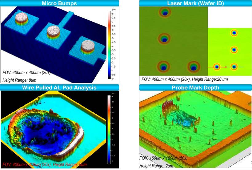
Semiconductor Related Samples
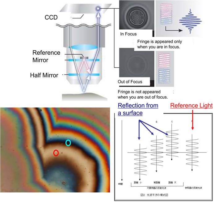
Principle
Focus Variation with White Light Interferometer
- Light is divided into 2 optical paths at Half Mirror. One is Reference path and another is Reflection path from a surface.
- Reflection path is delayed based on sample surface unevenness.
Reflection and Reference at Red Point.
wave length at Blue Point.
|


System Overview
Specification Overview |
|
Base unit | OST3100 Base ( 1 LP) |
Functions | - Conventional Microscope Observation & Image Capturing - Precision height and roughness measurement - Creating wafer map, recipe and automatic measurement including Auto Focusing and Enhanced Global Alignment. |
Applications | - 200/300mm micro bump, redistribution lines and cu pillar. - TSV and MEMS |
Wafer size | 200mm and 300mm |
Wafer thickness | 400um ~ 1,500um |
Wafer warped volume | Less than 800um (Need to evaluate) |