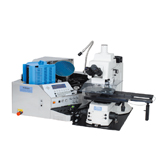
Nikon NWL - 200 / 8" 6" Wafer Inspection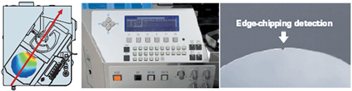 Nikon’s outstanding proprietary technology makes the NWL - 200 Series the first lineup of wafer loaders for inspection microscopes capable of loading 100μm thin wafers(Bare wafer). The NWL - 200 Series achieves highly reliable loading suitable for inspection of next-generation semiconductors.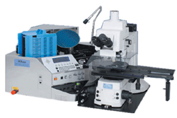 • Available for 5"",6"",8"" wafer inspection by different recipe(5"" Option). |
Nikon NWL - 200 / 8" 6" Wafer Inspection
Nikon’s outstanding proprietary technology makes the NWL200 Series the first lineup of wafer loaders for inspection microscopes capable of loading 100μm thin wafers(Bare wafer) . The NWL200 Series achieves highly reliable loading suitable for inspection o
服務據點
台北總公司
105台北市松山區南京東路三段272號8樓
Tel:(02) 2740-3366
Fax:(02) 2773-5577
新竹分公司
300新竹市東區關新路27號15樓之2
Tel:(03) 564-1360
Fax:(03) 564-1363
台中分公司
406台中市北屯區文心路四段450號
Tel:(04) 2230-0077
Fax:(04) 2230-0055
台南分公司
744台南市新市區光明街82號
Tel:(06) 589-1721
Fax:(06) 589-1728
高雄分公司
806高雄市前鎮區民權二路8號12樓之2
Tel:(07) 537-3990
Fax:(07) 537-3880